Select the executable file link to download the file to your hard disk. Single port Read Only Memory ROM Read Only Memory ROM is a constant memory.
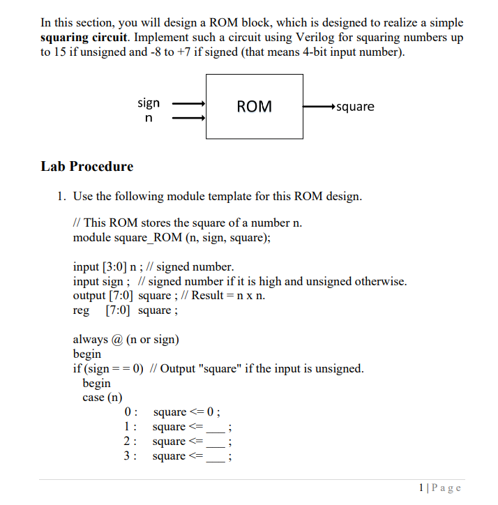
In This Section You Will Design A Rom Block Which Chegg Com
Design hierarchy also plays an important role in designing the basic building blocks required in each step of verification.

. Following is the figure and verilog code of ROM Read Only Memory. As you state the coefficients will be stored in a RAM LUT or in a ROM block. Use synopsys to run files and show the output.
Sectionlabel FMS design is known as Moore design if the output of the system depends only on the states see Fig. Introduction to XILINX and MODELSIM SIMULATOR httpsyoutubey9fL7ahhwn0 FULL ADDER USING HALF ADDER IN VERILOGhttpsyoutube9uIJEmqeMrw RIPPLE CARRY. ROM in verilog If you use ROM for emulation you can use this construct for example.
A Verilog HDL synthesis attribute that specifies the type of TriMatrix Memory block to use when implementing an inferred ROM in your design. Low Pass FIR Filter Asynchronous FIFO design with verilog code D FF without. Whether it is a ROM or RAM.
The Verilog does not have user-defined types and we are restricted to arrays of built-in Verilog types such as nets regs and other Verilog variable types. Reg 310 my_rom 01023. ROM in verilog Setting the ROM content in an initial block is the exact equivalent to the VHDL initialized signal and should work with any device that has ROM.
Look for Inferring ROM section in iCEcube2. To introduce the Verilog programming. A simple memory is implemented using.
6111 Spring 2006 Introductory Digital Systems Laboratory 8 Block RAMROM Contents coe file looks like. Digital Design An Embedded Systems. The code is somewhat self-descriptive the always is sensitive to the address then each time the.
ROM can be used to hold initial data for. Verilog RAM RTL code. Here the memory is 80 bit wide and with a depth of 16.
The Quartus II software supports this synthesis. Synchronous Random Access Memory RAM implementation in Verilog. You can implement something as follows broad view pseudo-codeHere mem0 is least address block and each block has 0th bit as.
Mealy and Moore designs. Two dimensional arrays can not be at port inputoutput in Verilog. In previous chapters some simple designs were introduces eg.
Each section shows the list of Verilog-files require to implement the design in that section. This page contains Verilog tutorial Verilog Syntax Verilog Quick Reference PLI modeling memory and FSM Writing Testbenches in Verilog. Take a note of a synthesis attribute rom_style block which instructs the synthesis tool how to infer ROM memory.
Design module single_port_sync_ram parameter ADDR_WIDTH 4 parameter DATA_WIDTH 32 parameter DEPTH 16 input clk input ADDR_WIDTH-10 addr inout DATA_WIDTH-10. 1 ----- 2 Design Name. The usage of this type of memory is obvious.
In this project we design a 64-bit x 8-bit which is a single. So the address width must be log216 4 4 bits wide. But they can be declared and used within inside module.
Intel provides Verilog HDL design examples as downloadable executable files or displayed as text in your web browser. Not clear how does it tie to havingnot having a package at the first place. Assign rd rom addr.
Specify input radix memory_initialization_radix2. Mod-m counter and flip-flops etc. Home Interview Basics Design RTL VLSI Python LTE.
To use the romstyle attribute in a Verilog Design File v Definition specify the synthesis attribute in a comment following the Variable Declaration of an. Module ROM_codeout addr CS.
Design Of Rom In Verilog Youtube

Verilog Tutorial 05 Simple Rom Youtube

Verilog Tutorial 05 Simple Rom Youtube

Verilog Code For Rom Youtube

Modelling Of Memory Part 2 Modelling Read Only Memory Rom Verilog Part 25 Youtube

Ram Verilog Code Rom Verilog Code Ram Vs Rom

Ram Verilog Code Rom Verilog Code Ram Vs Rom

Pin Auf Books
0 comments
Post a Comment